Posts

Showing posts from November, 2021

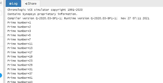
Vedic Multiplier Design

8x8 Vedic Multiplier using Ripple carry adder and 4x4 multiplier module vedic8x8( input [7:0] a,b,  output [15:0] prod ); wire [7:0] mult0, mult1, mult2, mult3; wire [7:0] sum0; wire [11:0] sum1, sum2; wire carry0, carry2, carry3; vedic4x4 VM_i0(a[3:0],b[3:0],mult0); vedic4x4 VM_i1(a[3:0],b[7:4],mult1); vedic4x4 VM_i2(a[7:4],b[3:0],mult2); vedic4x4 VM_i3(a[7:4],b[7:4],mult3); ripple_adder_8bit RA_i0({4'b0,mult0[7:4]},mult2,1'b0,sum0,carry0); ripple_adder_12bit RA_i1({4'b0,mult1},{mult3,4'b0},1'b0,sum1,carry1); ripple_adder_12bit RA_i2({4'b0,sum0},sum1,1'b0,sum2,carry2); assign prod = {sum2,mult0[3:0]}; endmodule 4x4 Vedic Multiplier using Ripple carry adder and 2x2 multiplier module vedic4x4( input [3:0] a,b,  output [7:0] prod ); wire [3:0] mult0, mult1, mult2, mult3; wire [3:0] sum0; wire [5:0] sum1, sum2; wire carry0, carry1, carry2; vedic2x2 VM_i0(a[1:0],b[1:0],mult0); vedic2x2 VM_i1(a[1:0],b[3:2],mult1);

Program in HDL to generate nth Fibonacci number Where n is the input?

Image
`timescale 1ns / 1ps ////////////////////////////////////////////////////////////////////////////////// // Company: Weekendvlsi.blogspot.com // Engineer: Weekendvlsi //  // Create Date: 27-11-2021 // Design Name:  // Module Name:  // Project Name: Printing nth Fibonacci // Target Devices:  // Tool Versions:  // Description:  //  // Dependencies:  //  // Revision: // Revision 0.01 - File Created // Additional Comments: //  ////////////////////////////////////////////////////////////////////////////////// module nth_fibonacci_num( input clk,  input rst,   input [7:0] nth_fibonacci_req, output [19:0] nth_fibonacci_value     ) ;  reg [19:0] previous_value, present_value;     reg [7:0] ctr;     reg output_valid;  assign nth_fibonacci_value = present_value ; always @( posedge clk) begin         if (rst) begin             previous_value   <=0;              present_value    <=1;              ctr <=1;         end         else begin                       if (ctr == (nth_fibonacci_req-1)

Prime Number Detection

Image
  Prime Number Detection: `timescale 1ns / 1ps ////////////////////////////////////////////////////////////////////////////////// // Company: Weekendvlsi.blogspot.com // Engineer: Weekendvlsi // Create Date: 27-11-2021 // Design Name: Prime Number Detection // Module Name: prime_number // Project Name:  // Target Devices:  // Tool Versions:  // Description:  // Dependencies:  // Revision: // Revision 0.01 - File Created // Additional Comments: //  ////////////////////////////////////////////////////////////////////////////////// module prime_number ( input clk,  reset) ;   parameter N =50;          // size of array   reg [31:0] dump[0:N-1]; // memory array for product          integer i=0 ;                  integer result_done =1;        integer count =0;        always @(posedge clk )       begin      if(reset)       for(i=0;i<N;i=i+1)       begin          dump[i]='d0;       end           else begin          count = count+1 ;       if ((count%2==0 && count!=2) || (count%

RTL Design Interview Questions

  Explain the difference between synchronous and asynchronous FIFO designs and their uses. Can you design a parameterized 2:1 multiplexer? Explain the difference between these three versions of Verilog case statement: cases, casez and case-inside. Also, when do you use these as an RTL engineer? What do you do at the RTL level to meet timing in synthesis? Provide an example. What's the difference between SRAM and DRAM? Difference between Latch and Flipflop? What are two ways of converting a two-input NAND gate to an inverter? write a code for edge detector ? Can you tell me about the engineering design process? Explain how to quickly identify whether a number is a power of 2. What's a unary operator? Setup time and Hold Time ? Design NAND Gate Using 2:1 Mux? Design Flipflop using Latch? Difference between Blocking and Non Blocking Statements ? Explain Parallel and Sequence Statements? Explain ASIC and FPGA Difference ? What is Meta Stability? Design XOR from NAND gates?  Design

Number of one's Detection in Input - Verilog Implementation

Image
  Number of one's Detection: `timescale 1ns / 1ps ////////////////////////////////////////////////////////////////////////////////// // Company: Weekendvlsi.blogspot.com // Engineer: Weekendvlsi // Create Date: 20-11-2021 // Design Name: Number of one's Detection // Module Name: num_ones  ////////////////////////////////////////////////////////////////////////////////// module num_ones(     input [15:0] In,     output reg [5:0] ones_detect     ); integer i; always@(In) begin      ones_detect= 0;       for(i=0;i<16;i=i+1)    begin          if(In[i] == 1'b1)             ones_detect = ones_detect + 1;     end end endmodule TEST BENCH: module tb;   reg  [15:0] In;   wire  [5:0] ones_detect;    num_ones dut ( In,ones_detect);    initial begin           In=16'h1212;     #50   In=16'h2021;     #50   In=16'h1112;     #50   In=16'h2010;    #300  $stop;        end    initial begin      $dumpfile("dump.vcd");     $dumpvars;   end   endmodule  RESUL

Weekend VLSI HOME

    Weekend VLSI   About Us :  Struggling a lot to enter into the VLSI Industry? We too went through this phase, Trust us and do work hard. If we can get into Industry, YOU TOO CAN . To help you, we come up with this blog. It's in initial phase, We'll keep gathering information and place it in front of you in Simple terms. Also give use some feedbacks or the topics you are interested and want to know further, We'll post on that as well.  VLSI COMPANIES LIST RTL CODING GUIDE LINES RTL coding Guide Lines DIGTIAL ELECTRONICS QUESTIONS   Digital Electronics Questions   RTL DESIGN QUESTIONS RTL Design Questions RTL CODING EXAMPLES Vending Machine With Display options Different ways to Design ROM   6 bit Full adder Using 3 bit Full adder   3 bit Subtractor  Post Divider 4x4 Booth Multiplier 101101 Sequence Detector Falling Edge Detector Rising Edge Detector FIFO Number of one's Detection In Input Prime Number Fibonacci Number 8x8 Vedic Multiplier Rational Clock Division   Di

RTL Guide Lines

Guideline 1 : Need to state all the conditions else un-intentional latches will come up. Example : case (x,y) 00,01: z=1; 10: z=0 ; //11 case will infer a latch which isn't required endcase Guideline 2 : Perfect synchronization should be maintained for the external world signals coming into the chip. Guideline 3 : Have a good knowledge on CDC and double check the signals going through multiple clock domains. Guideline 4 : Don't mix up Blocking and Non Blocking statements in an always block. Always know the differences netween blocking and non blocking assignments. Guideline 5 : It is always suggested to seperate combinational and sequential logic. Guideline 6 : Have an idea of where to use reg and where to use wire. Guideline 7 : To design a synthesizable logic, know the synthesizable keywords and use it properly. Guideline 8 : The sensitivity list of a combinational always block must include all the inputs used in that block. If you forget some signals from the sensitiv

Digital Electronics Questions For VLSI Interview

Digital Electronics Questions For VLSI Interview   Which gates are called universal gates? Why? Define: (a) bit (b) nibble (c) byte (d) word What is weighted code? Give example.  Give an example for Non-weighted code .  What is the key feature of Excess-3 code? What is the condition for a weighted code to be self-complementary? Convert the binary number 011101010001 to octal and hexadecimal?How many number of 2 input AND gates are required to generate N I/P AND gate? State De-Morgan’s Laws? If it is given that A & B will not be 1 at the same time, what will be theequivalent logical gate for an XOR gate?  If any of the inputs of an XOR gate are inverted, XOR gate will work as ----- ? Give implementation of XOR using minimum number of NAND gates? Which logical gates can be used as parity generators? Which logical gate can be used to find out whether the two single bit inputs are equal or not?  What is the difference between NAND gate and negative AND gate? XOR gate can be used as eve

FIFO Design Using Verilog HDL

  FIFO (First In and First Out): `timescale 1ns / 1ps ////////////////////////////////////////////////////////////////////////////////// // Company: www.weekendVLSI.blogspot.com // Engineer:  www.weekendVLSI.blogspot.com     // Design Name:    FIFO // Module Name:    fifo_verilog  // Project Name:    FIFO ////////////////////////////////////////////////////////////////////////////////// module fifo_verilog(     input rst,     input clk,     input wr_en,     input rd_en,     input [7:0] wr_data,     output [7:0] rd_data,     output Memory_full,     output Memory_empty     ); reg [7:0]Memory_temp[15:0]; integer wr_index, rd_index; integer r_fifo_count = 0; wire w_full, w_empty; always @(posedge(clk)) begin   if (rst == 1) begin      wr_index=1'b0;   rd_index=1'b0;   r_fifo_count=0;    end    else begin       if (wr_en == 1'b1 && rd_en == 1'b0 && r_fifo_count < 16) begin r_fifo_count <= r_fifo_count + 1; end else if (wr_en == 1&#

Rising Edge Detector

Image
 Rising Edge Detector: `timescale 1ns / 1ps ////////////////////////////////////////////////////////////////////////////////// // Company: Weekendvlsi.blogspot.com // Engineer: Weekendvlsi // Create Date:  // Design Name: Rising Edge Detector // Module Name: pos_detect ////////////////////////////////////////////////////////////////////////////////// module pos_detect (output neg_det, input clk,rst,d);   reg  q,y;  always @(posedge clk  ) begin      if(rst)         q<=0;     else begin         q<=d;      end    end   not v1 (y,q);    and v2 (neg_det,y,d);  endmodule  RESULTS :                        

Falling Edge Detector

Image
 Falling Edge Detector : `timescale 1ns / 1ps ////////////////////////////////////////////////////////////////////////////////// // Company: Weekendvlsi.blogspot.com // Engineer: Weekendvlsi // Create Date:  // Design Name: Falling Edge Detector  // Module Name: neg_detect  ////////////////////////////////////////////////////////////////////////////////// module neg_detect (output neg_det, input clk,rst,d);   reg  q,y;    always @(posedge clk  ) begin      if(rst)         q<=0;     else begin         q<=d;     end    end   not v1 (y,d);     and v2 (neg_det,y,q);   endmodule  Result:

101101 Sequence Detector

Image
Code for detecting pattern from the Seq_in input. `timescale 1ns / 1ps ////////////////////////////////////////////////////////////////////////////////// // Company: Weekendvlsi.blogspot.com // Engineer: Weekendvlsi //  // Create Date: 20-11-2021 // Design Name:  // Module Name: pattern_detector // Project Name:  // Target Devices:  // Tool Versions:  // Description:  //  // Dependencies:  //  // Revision: // Revision 0.01 - File Created // Additional Comments: //  ////////////////////////////////////////////////////////////////////////////////// module pattern_detector(rst,clk,seq_in,pattern_detected); output reg pattern_detected;   input clk, rst, seq_in; reg [2:0] current_state; reg [2:0] next_state; parameter [2:0] state_0=3'b000; parameter [2:0] state_1=3'b001; parameter [2:0] state_2=3'b010; parameter [2:0] state_3=3'b011; parameter [2:0] state_4=3'b100; parameter [2:0] state_5=3'b101; always @(posedge clk, posedge rst) begin

Different Ways to Design Post Divider

Image
Method -1: module clk_divider ( input clk,rst, input [2:0] a, output reg f2,f4,f8,f16,f32,f64,f128 ); reg [6:0] q; always@(posedge clk, posedge rst) begin   if(rst)    f2=1'b0;    else begin     q[0]=~f2; if(a==3'b001) f2=q[0]; else f2=1'b0; end end always@(posedge q[0], posedge rst) begin   if(rst)    f4=1'b0;    else begin     q[1]=~f4; if(a==3'b010) f4=q[1]; else f4=1'b0; end end always@(posedge q[1], posedge rst) begin   if(rst)    f8=1'b0;    else begin     q[2]=~f8; if(a==3'b011) f8=q[2]; else f8=1'b0; end end always@(posedge q[2], posedge rst) begin   if(rst)    f16=1'b0;    else begin     q[3]=~f16; if(a==3'b100) f16=q[3]; else f16=1'b0; end end always@(posedge q[3], posedge rst) begin   if(rst)    f32=1'b0;    else begin     q[4]=~f32; if(a==3'b101) f32=q[4]; else f32=1'b0; end end always@(posedge q[4], posedge rst) begin   if(rst)    f64=

4X4 BOOTH MULTIPLIER

  4X4 BOOTH MULTIPLIER module BOOTH_Multiplier(RESULT, X, Y);   RESULT reg signed [7:0] RESULT;   input signed [3:0] X,Y;  reg [1:0] State;   reg [5:0] K;   reg e;   reg [3:0] Z;   always @(X,Y)   begin     RESULT = 8'd0;     e = 1'b0;     Z = -Y;          for (K=0; K<4; K=K+1)     begin       State = { X[K], e };       case(State)         2'd2 : RESULT[7:4] = RESULT[7:4] + Z;         2'd1 : RESULT[7:4] = RESULT[7:4] + Y;       endcase       RESULT = RESULT >> 1;       RESULT[7] = RESULT[6];       e=X[K];            end   end    endmodule

Vending machine Code With Display Options

Image
  Vending machine Top Module : module vending_machine_top (input                 clk,                                                     input                  rst,            input                  coin_valid,            input [2:0]         coin,            output                 cup_f,            output [375:0]   Display_out,           output  [5:0]      bal                                                  );     wire [2:0]   w_addr;     vending_machine   V1  (       .clk            (clk),                                                .rst              (rst),                .coin_valid (coin_valid),         .coin          (coin),           .cup_f       (cup_f),           .addr         (w_addr),          .bal            (bal)                                    );     Display          v2  ( .Display_out     (Display_out) ,                                  .addr                 (w_addr),                              

3 Bit Subtractor Using 1 bit Subtractor

Image
 1bit Subtractor : module full_sub_bit(Diff,Bout,A,B,BI); output Diff,Bout; input  A,B,BI;    wire x,x1,y,z,y2;   xor V1 (x,A,B),V2 (Diff,x,BI);     not V3 (y,A),v4 (x1,x);   and V5 (z,y,B),V6 (y2,x1,BI);   or   V7 (Bout,y2,z);  endmodule 3bit Subtractor : module full_sub_3bit (Sub, BO, A, B, BI,);   input [2:0] A, B;   input BI;   output [2:0] Sub;   output BO;   wire B1,B2;   full_sub_bit v1 (Sub[0],B1,A[0],B[0],BI);    (Module name  Instantiation name   Ports mapping);    full_sub_bit v2 (Sub[1],B2,A[1],B[1],B1);    full_sub_bit v3 (Sub[2],BO,A[2],B[2],B2);   endmodule  TESTBENCH module tb;   reg  [2:0] A,B;   reg  BI;     wire [2:0] Sub;   wire BO;     full_sub_3bit dut  (Sub, BO, A, B, BI,);      initial begin         A=3'b000; B=3'b100; BI=0;     #1 A=3'b000; B=3'b010; BI=1;     #1 A=3'b101; B=3'b001; BI=0;     #1 A=3'b110; B=3'b011; BI=1;     #1 A=3'b000; B=3'b110; BI=1;     #1 A=3'b111; B=3'b001; BI=0;     #1 A=3'b110; B=3